• Skip to primary navigation
  • Skip to main content
  • Skip to primary sidebar
  • Skip to secondary sidebar
  • About
    • Contact
    • Privacy
    • Terms of use
  • Advertise
    • Advertising
    • Case studies
    • Design
    • Email marketing
    • Features list
    • Lead generation
    • Magazine
    • Press releases
    • Publishing
    • Sponsor an article
    • Webcasting
    • Webinars
    • White papers
    • Writing
  • Subscribe to Newsletter

Robotics & Automation News

Where Innovation Meets Imagination

  • Home
  • News
  • Features
  • Editorial Sections A-Z
    • Agriculture
    • Aircraft
    • Artificial Intelligence
    • Automation
    • Autonomous Vehicles
    • Business
    • Computing
    • Construction
    • Culture
    • Design
    • Drones
    • Economy
    • Energy
    • Engineering
    • Environment
    • Health
    • Humanoids
    • Industrial robots
    • Industry
    • Infrastructure
    • Investments
    • Logistics
    • Manufacturing
    • Marine
    • Material handling
    • Materials
    • Mining
    • Promoted
    • Research
    • Robotics
    • Science
    • Sensors
    • Service robots
    • Software
    • Space
    • Technology
    • Transportation
    • Warehouse robots
    • Wearables
  • Press releases
  • Events

Fraunhofer develops ‘resource-efficient’ measurement system for semiconductor wafer production

July 17, 2025 by David Edwards

The Fraunhofer Institute for Photonic Microsystems (IPMS), in collaboration with DIVE imaging systems, has achieved a major milestone in resource-efficient semiconductor manufacturing.

With the successful installation of an optical measurement system by DIVE in the cleanroom of Fraunhofer IPMS, the effort required for quality control during wafer production has been significantly reduced. This collaboration paves the way for a more sustainable and efficient semiconductor production process.

Semiconductor manufacturing involves up to 1,500 process steps, including etching, deposition and lithography. Due to their complexity of structures, finished wafers must be nearly defect-free, which requires rigorous quality control.

As a result, up to 50 percent of process steps are dedicated to metrology and thousands of additional control wafers are produced each month. This requires substantial additional financial and material expenditures as well as energy and time resources.

The project “NEST” (New Screening Tool for Efficient Semiconductor Manufacturing) directly addresses this issue. Over the past 1.5 years, DIVE, together with Fraunhofer IPMS and Fraunhofer IZM has conducted an environmental potential analysis.

The study revealed that targeted inspection tools could reduce control wafer usage by at least 25 percent, while also saving more than 118,000 kilograms of CO₂ emissions during production every month.

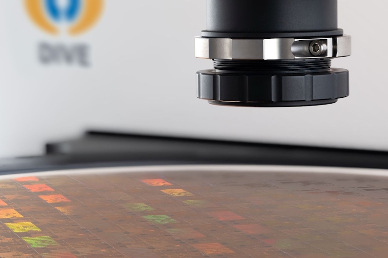
DIVE’s solution uses an innovative combination of spectroscopy and imaging technologies capable of identifying defects even in deeper wafer layers.

The analysis was based on a 28 nm manufacturing process and 25,000 wafer starts per month. The project was funded within the “Green ICT Space” by the Research Fab Microelectronics Germany (FMD).

In addition to CO₂ savings, the system offers further ecological benefits, such as the reduction of water and chemicals used in control wafer production.

Furthermore, the reduction of metrology steps also improves energy efficiency by freeing up tool capacity; an early detection of process deviations avoids misproduction and improves the overall productive wafer yield, which results in an economic advantage as well.

Industry-ready evaluation in cleanroom environment at Fraunhofer IPMS

DIVE imaging systems develops advanced inspection tools that combine the benefits of optical spectroscopy with imaging. The DIVE VEpioneer is the first of its kind to operate under cleanroom conditions. It rapidly assesses surface properties, contamination and deviations from production specifications in just 20 seconds.

The integration of AI algorithms enables comprehensive process control while significantly reducing testing efforts. “DIVE’s hyperspectral imaging systems offer a new way of non-destructive wafer inspection.

With the support of Fraunhofer IPMS, this innovative technology is now available for use in standardized industrial cleanrooms – enabling significant productivity gains and cost savings for semiconductor fabs,” says Martin Landgraf, R&D Manager at Fraunhofer IPMS.

After the successful conclusion of the project, the DIVE VEpioneer system will remain at Fraunhofer IPMS’s Center Nanoelectronic Technologies (CNT) for continued wafer measurement and evaluation for customers and partners.

Further joint projects are planned to enhance the system with wafer handling automation and equipment integration for an automatic data transfer.

With the acquisition of DIVE imaging systems by PVA TePla AG, the start-up now gains new opportunities for evaluation and development – particularly through the expertise of the material and metrology specialist.
Print Friendly, PDF & Email

Share this:

  • Click to print (Opens in new window) Print
  • Click to share on Facebook (Opens in new window) Facebook
  • Click to share on LinkedIn (Opens in new window) LinkedIn
  • Click to share on Reddit (Opens in new window) Reddit
  • Click to share on X (Opens in new window) X
  • Click to share on Tumblr (Opens in new window) Tumblr
  • Click to share on Pinterest (Opens in new window) Pinterest
  • Click to share on WhatsApp (Opens in new window) WhatsApp
  • Click to share on Telegram (Opens in new window) Telegram
  • Click to share on Pocket (Opens in new window) Pocket

Related stories you might also like…

Filed Under: Features, Science Tagged With: cleanroom technology, co2 reduction, dive imaging systems, fraunhofer ipms, green ict, hyperspectral imaging, optical metrology, semiconductor manufacturing, sustainable chip production, wafer inspection

Primary Sidebar

Search this website

Latest articles

  • Construction and demolition robots: Building the future
  • Robotics Rising: What Hiring Trends Reveal About Automation Careers
  • Xpanner launches ‘first’ scalable physical AI-based automation solution for construction sites
  • Skelex starts exoskeleton pilot in greenhouses in the Netherlands
  • Humanoid Global makes ‘software investment’ in RideScan
  • $50 million funding sparks ‘manufacturing technology breakthroughs‘ in Ontario
  • Wachendorff expands range of IO-Link encoders
  • Robotics survey highlights autonomy, digital twins, humanoids and ethics as key 2025 trends
  • ABB to implement gearless mill drive service program at Codelco copper mines in Chile
  • Systraplan unveils new automatic tread booking systems for tyre manufacturing

Secondary Sidebar

Copyright © 2025 · News Pro on Genesis Framework · WordPress · Log in

We use cookies on our website to give you the most relevant experience by remembering your preferences and repeat visits. By clicking “Accept”, you consent to the use of ALL the cookies.
Do not sell my personal information.
Cookie SettingsAccept
Manage consent

Privacy Overview

This website uses cookies to improve your experience while you navigate through the website. Out of these, the cookies that are categorized as necessary are stored on your browser as they are essential for the working of basic functionalities of the website. We also use third-party cookies that help us analyze and understand how you use this website. These cookies will be stored in your browser only with your consent. You also have the option to opt-out of these cookies. But opting out of some of these cookies may affect your browsing experience.
Necessary
Always Enabled
Necessary cookies are absolutely essential for the website to function properly. These cookies ensure basic functionalities and security features of the website, anonymously.
CookieDurationDescription
cookielawinfo-checkbox-analytics11 monthsThis cookie is set by GDPR Cookie Consent plugin. The cookie is used to store the user consent for the cookies in the category "Analytics".
cookielawinfo-checkbox-functional11 monthsThe cookie is set by GDPR cookie consent to record the user consent for the cookies in the category "Functional".
cookielawinfo-checkbox-necessary11 monthsThis cookie is set by GDPR Cookie Consent plugin. The cookies is used to store the user consent for the cookies in the category "Necessary".
cookielawinfo-checkbox-others11 monthsThis cookie is set by GDPR Cookie Consent plugin. The cookie is used to store the user consent for the cookies in the category "Other.
cookielawinfo-checkbox-performance11 monthsThis cookie is set by GDPR Cookie Consent plugin. The cookie is used to store the user consent for the cookies in the category "Performance".
viewed_cookie_policy11 monthsThe cookie is set by the GDPR Cookie Consent plugin and is used to store whether or not user has consented to the use of cookies. It does not store any personal data.
Functional
Functional cookies help to perform certain functionalities like sharing the content of the website on social media platforms, collect feedbacks, and other third-party features.
Performance
Performance cookies are used to understand and analyze the key performance indexes of the website which helps in delivering a better user experience for the visitors.
Analytics
Analytical cookies are used to understand how visitors interact with the website. These cookies help provide information on metrics the number of visitors, bounce rate, traffic source, etc.
Advertisement
Advertisement cookies are used to provide visitors with relevant ads and marketing campaigns. These cookies track visitors across websites and collect information to provide customized ads.
Others
Other uncategorized cookies are those that are being analyzed and have not been classified into a category as yet.
SAVE & ACCEPT